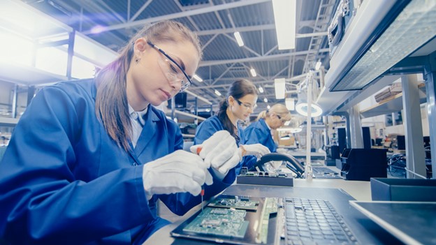
The team at OBMFG understands the importance and impact of PCBs. Electronic devices used today have cores that are formed mainly by Printed Circuit Boards (PCBs). Everything from cars to refrigerators to smartphones has electronics with these modern components found online or in some specialized retailers. The PCB is the foundation onto which a variety of small electrical components are attached. The process of mounting the right components for an application to a blank PCB and then testing and inspecting the board is called PCB Assembly.
As the demand for more functionality in electronic devices continues to soar and we advance these technologies to meet industrial and consumer needs, more complex and smaller PCBs and components are being designed and produced. For this reason, the PCB assembly process has become an even more critical step in electronics manufacturing. One small assembly error could lead to the failure of a component, impacting the customer experience or safety.
Given how important this process has become, having an experienced PCB assembly partner should be a priority. Here is what you need to know about the different PCB assembly technology options and the vital steps in the PCB assembly process to make the right choice.
Different PCB Assembly Technologies
There are two primary ways to join components to a PCB - surface mount and through-hole.
-
 Surface Mount Technology (SMT) - This is the most widely-used technique. As you might imagine, SMT involves attaching components directly onto the surface of the PCB board. This is generally done by soldering. Since no holes are made in the board, components can be attached to both sides when necessary.
 -
 Through-Hole Technology (THT) - This technique involves drilling holes in the PCB board to attach various components. It helps make strong connections that can withstand heavy stress and vibrations. But it's not used as frequently as SMT.
Essential Steps in the PCB Assembly Process
Before the PCB assembly process begins, all of the right design elements must be in place. Also known as a DFM (Design for Manufacturability) Check, this process reviews the design specifications and verifies that nothing is missing, there aren't any problem areas or any unnecessary redundancies. This step before the PCB assembly process can help eliminate any unforeseen delays or expenses.
Once complete, the actual steps in the PCB assembly process include:
- Solder Paste Stenciling
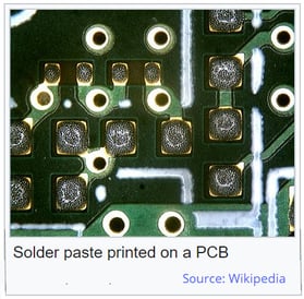 The first step of PCB assembly involves adding a solder paste to the PCB board on the areas where the components will be secured. The PCB board and a stainless-steel stencil are held together mechanically. Then, solder paste is applied by an applicator evenly across the openings in the stencil. When the solder paste dries, and the two components are separated, the paste remains only on the desired areas of the PCB board.
The solder paste is a greyish substance composed of 96.5% tin, 3% silver, and 0.5% copper. The composition of the paste is designed to quickly bond and melt to a surface when applied properly.
- Pick and Place of Components
After the solder paste is applied to the PCB board, the assembly process moves to the next step, the pick and place machine. A robotic device will automatically place the required components on the board. Using the provided design-level file, the robot refers to the specific X & Y coordinates for every component required and accurately places them on the PCB board on top of the solder paste.
Before robotic pick and place machines were developed, a technician would complete this task using a set of tweezers. As you can imagine, this was prone to error and a time-consuming process. Now that technology has advanced, robots can complete these tasks 24/7 with absolute accuracy.
- Reflow Soldering
Once the required components are set, the third step in the PCB assembly process is called reflow soldering. This involves placing the entire PCB board and its components on a conveyer belt. The belt then moves the items into a large oven heated to a 250 degree C temperature so that the existing solder can melt. Once the solder melts, it affixes the components to the PCB board.
After its time in the oven, the assembly goes into a cooler, where it is slowly cooled to create a permanent joint between the PCB board and the various components. If you have a double-sided PCB board, the side with the smallest or fewest components will be treated first from steps one through three, and then the process is repeated for the other side.
- Inspection and Quality Control
The next step is to inspect and test the assembled board. Parts can move during the reflow process, which can impact connectivity or there might be misplaced components in some rare instances. Checking for these types of errors can involve several different types of inspections:
-
- Manual checks- An in-person visual inspection is performed to verify the quality of the PCB.
- Optical inspection- An automatic optical inspection (AOI) machine employs high-powered cameras to inspect the soldered connections.
- X-ray inspection- Used with more complex PCB assemblies, an X-ray machine will review the different layers of the PCB to identify any trouble spots.
Having high-quality control standards is vital at this stage because items that fail to pass inspection can be scrapped or reworked until all issues are resolved.
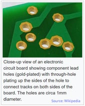
- Through-Hole Component Insertion
Some PCB boards also have through-hold components. The leads will often pass through a hole in the PCB assembly, and the different holes are interconnected using copper traces. Reflow assembly isn't effective when these through-hole technologies (THT) components are added to the PCB assembly. There are two primary methods for accomplishing through-hole assembly:
-
- Manual soldering- This generally involves one technician placing the components on the PCB board and another technician placing the next component, and so on.
- Wave soldering - is an automated version of manual soldering, where the components are added by a robotic device and then soldered all at once.
- Final Inspection and Function Test
Once this soldering process is complete, the PCB assembly process moves into its final stages before delivery. Final inspections and functional tests are performed where the assemblies are put in situations that mimic normal and peak circumstances to identify any unacceptable fluctuations. If a PCB fails the test, it is either scrapped or recycled.
- Final Cleaning, Finishing, and Shipment
Now that the PCB assembly has passed all inspections and tests, it can undergo a final cleaning before shipment. A high-pressure washing tool is used to remove any unwanted oil stains and residual dirt. Then, the assembly is dried using compressed air before careful packaging.
In the age of hyper-connectivity and smart devices, nearly everything we use contains a printed circuit board. Even though they remain invisible to most of us, how they are assembled is vital to the user experience and your business's bottom-line results.
Now that you understand the essential steps in the PCB assembly process, you can choose the best partner.
Out of the Box Manufacturing uses ISO-certified processes, fully-automated systems, expert engineering, and highly-trained production technicians to ensure that PCB assemblies are created right every time.
To learn more about our services and our commitment to excellence, contact us today.