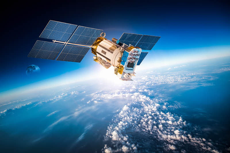
PCBs, or Printed Circuit Boards, are integral components of satellites and numerous other electronics. They provide the mechanical structure and electrical interconnections for their host electronic components.
In the context of satellites, PCBs are used in various subsystems such as communications, telemetry, power, propulsion, attitude determination, and control.
The following is a detailed description of the unique characteristics, components, and manufacturing considerations for PCBs used in satellites:
1) Materials: Satellites are exposed to harsh conditions like extreme temperatures, radiation, and microgravity. Thus, PCBs for satellites require unique materials. High-temperature laminates such as polyimide and cyanate ester are often used because of their resistance to thermal expansion. They also need to have low outgassing properties to prevent contamination in the vacuum of space.
2) Design: The design of PCBs for satellites is highly complex. They need to accommodate a multitude of components in a very constrained space. Additionally, the PCB design must prioritize weight reduction due to the high cost of launching weight into space. Multilayer PCBs are commonly used due to their compact size, despite the increased complexity in manufacturing and testing. They allow for multiple circuit layers stacked on each other, which can be interconnected using vias.
3) Components: Components mounted on these PCBs include microprocessors, memory, analog to digital converters, power supply components, RF modules, and sensors. Given the harsh operating conditions, these components should have radiation-hardened versions, i.e., resist damage from high-energy particles.
 4) Manufacturing and Testing: Due to the high-reliability requirements, satellite PCBs are manufactured and tested following stringent standards. This can include IPC Class 3 for high reliability or even more rigorous standards specific to space applications.
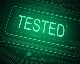
More about Testing a Printed Circuit Board (PCB) – Testing for satellites involves various stages, each designed to ensure the board will perform as expected in harsh space conditions. This involves electrical and environmental testing to simulate the conditions the PCB will face once it's in orbit. Here is a general outline of the process:
-
- Design Verification: Before the board is even built, computer simulations thoroughly verify its design. This includes checking for electrical design errors, verifying signal integrity, and conducting thermal analysis.
- Pre-manufacturing Testing: A bare board test is performed once the PCB design has been finalized. This usually involves an Automated Optical Inspection (AOI) or a computer-controlled scanning method that checks the board for manufacturing defects like shorts or opens, missing or excess copper, and correct hole sizes and locations.
- Post-assembly Inspection: After the components have been assembled on the PCB, it undergoes another round of inspections. This can include another AOI to check for missing or misplaced components, solder joint inspection, and X-ray inspection for detecting hidden solder defects.
- Electrical Testing: The PCB is then electrically tested to ensure it performs as expected. This can include continuity testing, functional testing, where the PCB is tested under operating conditions, and boundary scan testing, where integrated circuits are tested for correct operation.
- Environmental Testing: Since the PCB will be exposed to harsh conditions in space, it must undergo a series of environmental tests. These can include:
- Thermal Cycling: The PCB is exposed to extreme hot and cold temperatures to test its reliability under thermal stress.
- Vibration Testing: This test simulates the intense vibrations the satellite will experience during launch.
- Shock Testing: Simulates the mechanical shocks that can occur during the launch and deployment of the satellite.
- Vacuum Testing: Tests the PCB's ability to operate in the vacuum of space.
- Radiation Testing: Simulates the high-energy particles the PCB will be exposed to in space.
- Final Acceptance Testing: This is the final electrical and functional test before the PCB is integrated into the satellite. This verifies that the PCB is still operational after all the environmental testing.
- System-level Testing: Once the PCB has been integrated into the satellite, the system is tested to ensure all subsystems work together correctly. This can also include additional environmental testing of the whole satellite.
- Design Verification: Before the board is even built, computer simulations thoroughly verify its design. This includes checking for electrical design errors, verifying signal integrity, and conducting thermal analysis.
NOTE: PCB testing is typically conducted by the satellite manufacturer to ensure compatibility and ability to withstand extreme conditions.
5) Reliability and Redundancy: Since repair is impossible after launch, satellite PCBs must be extremely reliable. Design techniques like redundancy (where critical circuits are duplicated or even triplicated), error detection and correction in digital circuits, and derating (where components are operated at less than their maximum rated power) are used to enhance reliability.
6) Shielding: Satellites are exposed to a high level of radiation in space, which can cause damage to electronic components. PCBs used in satellites often feature shielding measures like conformal coatings or metal shielding to protect the components from radiation and prevent electrostatic discharge (ESD).
7) Thermal Management: PCBs in satellites must be designed to manage heat effectively since the usual convection-based cooling techniques do not work in the vacuum of space. Techniques like using thermal vias, heatsinks and selecting components that minimize heat generation are crucial.
Our team understands that PCBs in satellites are sophisticated pieces of technology that need to meet very stringent requirements due to the harsh space environment. Every aspect of their design, manufacturing, and steps in the process are meticulously controlled to ensure reliability and longevity.
What are typical problems from PCBs in satellites?
 Using Printed Circuit Boards (PCBs) in satellites involves some unique challenges due to the harsh environment of space. Typical problems encountered include:
Radiation Damage: Space is filled with high-energy particles, which can cause damage to the electronic components on a PCB. This can lead to a variety of issues, including
- Bit flips in memory
- Degradation of component performance over time
- Or, in extreme cases, complete failure of components.
Special radiation-hardened components mitigate these effects, but it's a constant challenge.
Thermal Management: In the vacuum of space, traditional heat dissipation methods, such as convection, do not work. This makes managing heat in PCBs particularly challenging. Excess heat can lead to premature failure of components. Engineers use various techniques to manage heat, including:
- Thermal vias
- Heatsinks
- And the careful selection of components to minimize heat generation.
Mechanical Stress: During the launch, intense vibrations and mechanical stresses can cause issues like solder joint fractures or component misalignment. These problems are typically addressed through robust design and extensive pre-launch testing.
Space Debris and Micro-meteoroids: Impacts from small particles can potentially cause physical damage to the satellite and its PCBs. While the risk is relatively low, and satellites are often shielded to protect against such impacts, it's a problem that needs to be considered.
Millions of naturally occurring micrometeoroids and man-made debris orbit the Earth. Orbital debris consists of remnants from previous missions. These items collide and explode creating additional pieces of debris that range from the size of a school bus down to the size of a grain of sand. These pieces of debris may seem innocuous but at hypervelocity speeds they can become killers.
Component Degradation: Over time, even radiation-hardened components can degrade due to the harsh conditions in space. This can lead to reduced performance and, ultimately, the failure of the satellite.
Limited Repair Options: Once a satellite is launched, repairing a faulty PCB is virtually impossible. This makes the design, manufacturing, and testing process extremely critical.
Outgassing: Some materials used in PCBs can release gases in the vacuum of space, a process known as outgassing. This can lead to contamination of other parts of the satellite and degradation of performance.
Size and Weight Constraints: Satellites have strict size and weight constraints, meaning PCBs must be as compact and lightweight as possible. This can make the design process more challenging, as fitting all the required functionality into a small package is necessary.
These are just some of the challenges engineers face when designing and manufacturing PCBs for satellites. Despite these challenges, technological advancements and manufacturing techniques continue to push the boundaries of what's possible.
We Assemble PCBs for Space
The Out of the Box Manufacturing team understands the complexities and strict requirements of PCBs in satellites. The extensive process and focus on quality ensure that PCBs withstand the most challenging environments, even space. Please take a moment to contact us to talk about your mission to space or ask for a quote!