
PCB Array Strength. This is the tradeoff between the ease of depanelization and array support during production. Increasing the board count per array can increase strength and reduce vibration, but there is a fine line. In this column, I will describe what is necessary to ensure you maximize the number of PCBs in the array and still provide adequate support strength for assembly.
Lately, we have seen an influx of PCBs that do not meet our needs to process the boards effectively. The repercussion of this is not being able to meet our deadlines at the highest level of standards.
Considerations to ensure quality
Component layout - The placement of components and connectors can limit your panelization options. What can limit your options:
- Overhanging components and connectors.
- Location of sensitive SMT parts near the edge of the PCB.
- The Shape of the PCB
So, what are the advantages of proper panelization?
- Adding breakaway rails can give you space for tooling holes for automated testing and SMT placement.
- Mass Production - If you need to build a lot of boards, panelization will save you TIME and MONEY.
- Support for odd-form PCB Designs.
- Efficiency and Speed - From Paste printing to component assembly, soldering, and testing. It's faster and more efficient to process multiple PCBs at once.

Let's dive in—the first order of business - The basics.
Panel Design Target.
- Rails on all four sides. (For three fiducials on the rails, the typical fiducial size is 1mm with 2.5mm mask clearances.)
- Tooling holes on all four corners
TO SCORE OR NOT TO SCORE
You may score the parts if your PCB part is square or rectangular.
The criteria here is you can have NO overhanging parts on the edge in question and must set any features or parts a minimum of .050" away from the scored edge.
However, suppose your PCB design has a combination of angles, radii, and flat edges that you wish to score. In that case, you will want to panelize them as a combination SCORE/ROUT where tabs and the flat sides will support the radii, and angles will be scored.
If your PCB design is odd form, it is essential to design your panelization to eliminate open space within the panel design. Automated processing equipment uses optical sensors to locate the PCB; open spaces often cause processing errors, creating unexpected downtime.

Now let's talk about TAB ROUT:
Tab sizes
The width of the tab will vary depending on the thickness of the dielectric.
As a rule of thumb, the tab width should be approximately 1.5 X the thickness (for example, .062 thick material would have approx.. .1" tab width. If unsure, consult your PCB MFG or IPC for the appropriate tab size.
Tab Perforations (Holes)
The hole size chosen for the tab breakaway is crucial for proper support and de-paneling. Perforation holes that are too large with too little material space between the perforations leave the array flimsy and susceptible to lack of support. The too-small size of perforation holes will make breaking the assemblies out difficult. Your PCB Manufacturer should have a guideline for the best design given the PCB specifications.
Tab locations
Your PCB fabricator should have suggestions for you based on overall PCB dielectric and PCB shape as to the best location of tabs. As a rule of thumb, a tab should be located approximately every 2.5".
Tabs should not be located where a component may overhang. The PCB manufacturer must be aware of any components that overhang to help them supply the best possible design. This will help them determine where you place tabs or routes.
Now, let's talk about the specific examples I will be focusing on.
Examples include: 1) Rails are not adequate. 2) The support is not effective. 3) Tabs are too small. 4) Bad arrays vs. Good arrays. 5) Not enough tabs, Rout too long without support.
My objective is to help you help us give the best product and services possible, here are examples to think more about your design, sources, and processes:
Example #1 - The rails are not adequate.
If the rails are less than .5" (.24" in the screenshot below), offset the fiducial marks in the rail inboard (towards the PCB) so the rail grabber on the SMT machines does not bury the fiducial.
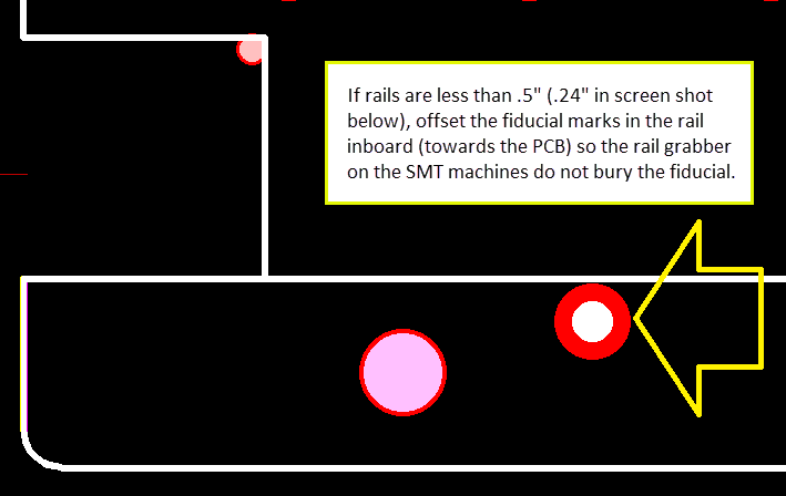
"The rails are not adequate." – The Fix.
Rail size on a given array should be .5" ideally for assembly. Anything less than .5", such as the .25 rails in the screenshot example #1, should have the rail fiducial offset inboard towards the PCB edge to make sure the rail grabber on the SMT machine does not bury the fiducial. This is an excellent example of a way to make a rail size smaller and still make it work for assembly.
Example #2 – The support is not effective.
In a continuous cut with NO tabs, the original route path on the panel Gerber's would completely sever the tooling and fiducials from the PCB array. Most likely, this was noticed, and two .1 tabs with 2 x .018 perf holes equidistantly spaced.
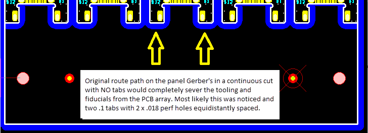
"The support is not effective." – The Fix.
Here, we have an array that is an example of UNSUPPORTED rails—understanding that the array rails typically have tooling holes (x4) and fiducials (x3) so an unsupported rail structure such as the one depicted in example #2 with rails on two edges ONLY and tabs way too small to support the rails resulted in PCB arrays that were broken off prematurely and would not have survived the stress created by the SMT process.
Example #3 - The tabs are too small.
Insufficient tabs are holding the board to the rail. Here, the route track comes from down the right-hand side, makes the corner, and severs the tab to the perforation holes, leaving approximately .020" remaining tab. (This is insufficient for support.)
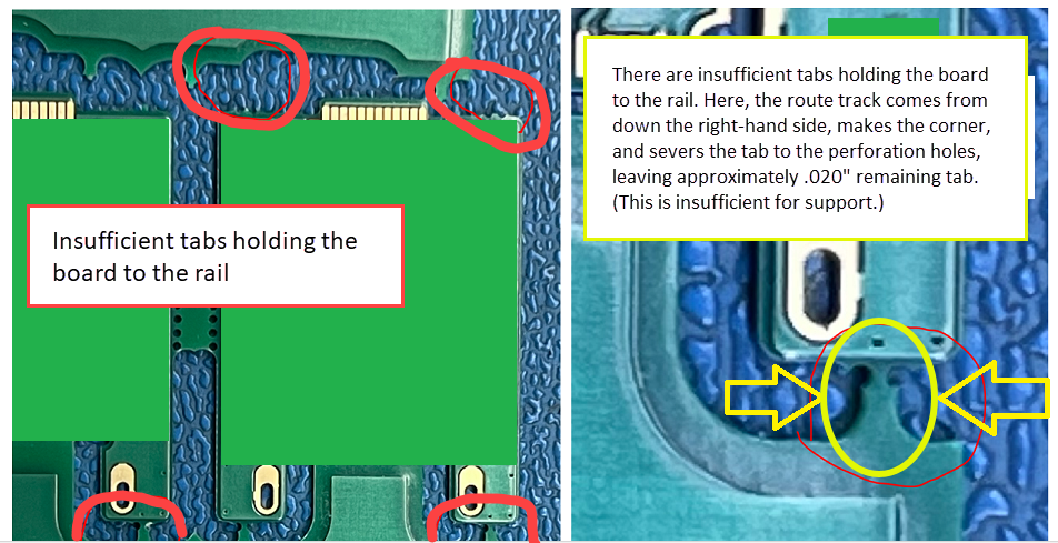
"- tabs are too small." – The Fix
This example was poorly designed.
1st - The tabs should have been on the sides without any features, not the sides with the edge and close edge features in the first place.
2nd - Realizing the original array only had perf tabs on one side left the entire array very flimsy, and any twisting at all would break the array, so the additional tabs on the ends near the edge features were added, which is why I am guessing this was an afterthought.
3rd - poor tab design. The tabs have TWO perforation holes located at the EDGES of the tab, effectively reducing the material to support the rails from .060" to .020", making it so flimsy the added rails broke off in shipping.
Example #4 - Bad arrays vs. Good arrays
BAD ARRAY – the original array Gerber
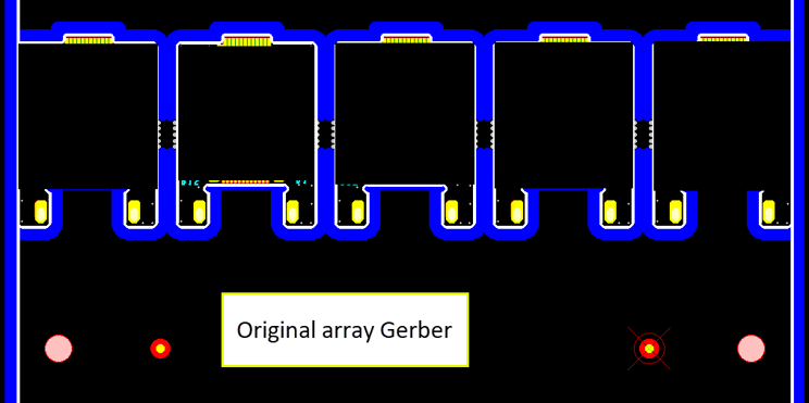
- GOOD - Green arrows show the new tab locations.
- BAD - Red arrows show the previous tab locations
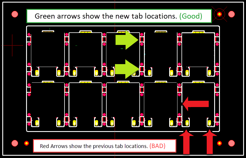
"Bad arrays vs. good arrays." – The Fix
A BETTER ARRAY
Here, the designer corrected the inadequacies of the previous array BOTH and kept the overall array size the same. Adding two tabs with perf holes on the sides closer to the corners could add the support needed and rout the edges with the close features cleanly and with no obstructions or protrusions.
Lastly, let's talk about minimum distances in example #5.
Example #5 - Not Enough tabs
Tabs should be placed at least every 2.5" to ensure the sub has support.
Something like the picture below results in rails that are floppy. For this, we would recommend the customer add tabs in TWO places.
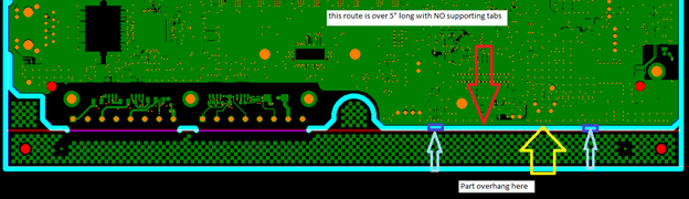
"Not enough tabs, Rout too long without support." – The Fix
Here, we have an example of a SCORE/ROUT where certain sections of the PCB are being scored, and other sections are being routed. Here are the takeaways:
1st - If your design has scored and routed sections, ensure balanced, symmetrical SCORED sections for equal support or add a tab on the routed sections for equal symmetrical support.
2nd - In example #5, score lines exist in sections with close edge features or edge connectors in the 1st half of the PCB length, but the second half is routed with NO additional tabs to support the rail. Here, another close-edge part exists about where a normal tab would exist. So, to have BOTH PCB support and still rout past the close edge feature, we recommend adding two tabs with perforation holes to support the second half of the length and balance the support. This unsupported rail is susceptible to movement, compromising part placement positional accuracy.
I hope this becomes a resource to ensure you receive the best from Out of the Box Manufacturing and other manufacturers. We have all been challenged in recent years, but our team continues to commit to excellence.
We Assemble PCBs
The Out of the Box Manufacturing team understands every industry's complexities and strict requirements for PCBs. The extensive process and focus on quality ensure that PCBs withstand the most challenging environments, even space. Please take a moment to contact us to talk about your mission or ask for a quote!
About the Author
 Mark Thompson C.I.D. - Sr. PCB technologist/ Engineering Manager
Mark has been in the engineering field for over 38 years. In 1993, he relocated to the Pacific Northwest, where he worked for Pacific Circuits, which became TTM, and Praegitzer Industries. He worked with Prototron from 1996–2019 and is now an engineering manager at Out of the Box Manufacturing.
He is passionate about his career, followed by aviation, art, and history. In his free time, Mark is an avid pilot, with a fondness for the aircraft of yesteryear. Mark says, "I have been privileged to fly many biplanes from the 1930s and 1940s, including Fleets, Stearmans, and N3Ns."
Mark enjoys sharing information and answering questions about PCB fabrication. Mark says: "The more information I can provide, the more fulfilled my customers and I will be."
Reach out to Mark here.